Semiconductor front equipment market: five giants control, Chinese manufacturers have a long way to go
The semiconductor has entered the atomic processing level, and the semiconductor device is manufactured in this accuracy, and more than 50 disciplines are needed. Moreover, the processing accuracy is only a dimension, and the yield is very important for semiconductor manufacturing. Therefore, both uniformity, stability, repetability, reliability and cleanliness are important. Advanced semiconductor processing links exceed 1000, which link has problems, it is difficult Make a chip that meets product performance and yield requirements.
Wen ︱ network
Figure ︱ network
According to the statistics of the market research institution SEMI, 2020 mainland China has become the world's largest semiconductor equipment regional market, and sales have increased by 39%, reaching 18.72 billion US dollars; China Taiwan ranked second, 2020 equipment sales in Taiwan Range of $ 17.15 billion; South Korea ranked 31% to $ 16.08 billion; Japan ranked fourth, sales also $ 7.58 billion. East Asia has become a global semiconductor army competition, 2020 comes 59.53 billion US dollars, accounting for 83.6% of the total global semiconductor equipment expenditure (US $ 71.2 billion).
Due to the influence of geopolitics to the semiconductor supply chain, in 2021 regional markets compete for semiconductor production capacity investment. TSMC and Samsung will adjust the capital expenditure of the semiconductor in the semiconductor to more than $ 30 billion in 2021. Two in advanced process production is expected to produce 3 nm technology in 2022, while the US government summoned , TSMC and Samsung will also go to the United States. There is no doubt that in 2021 will be a harvest year of semiconductor equipment manufacturers, while mainland China is subject to relevant restrictions, it is impossible to purchase equipment such as high-end EUV lightning machines, and stronger to hold the largest equipment market.
In the view of the Taiwan Industrial Research Institute (hereinafter referred to as Taiwan Institute of Technology), different regional markets are different from the development goals of the semiconductor industry: as the world's largest semiconductor application market, mainland China is in the context of supply chain security, it is undoubtedly more hope to speed up. Technology is champored to relieve the status quo of humanity in manufacturing, equipment and materials, etc.; the United States as the leader of the global semiconductor industry chain will continue to strengthen high-end chip manufacturing equipment to mainland China's export control, the United States will also introduce new politics To address the decline in the US wafer manufacturing capability in recent years; as the two regions of the global wafer manufacturing density, China Taiwan and South Korea will have hope to continue to lead the development trend of the wafer manufacturing process, these two areas will also be strong Manufacturing capabilities, improve the autonomous status of the upstream materials and equipment.
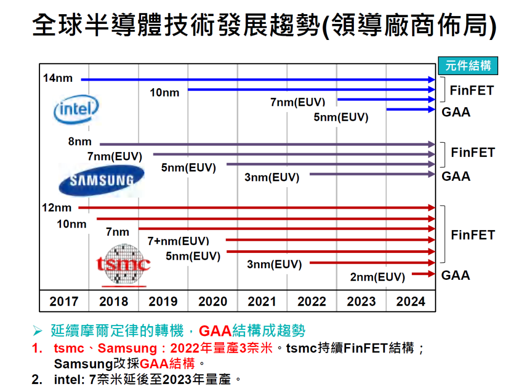
Advanced process development direction
After 28 nanometers, the planar transistor process reaches the limit, the FinFET (fin transistor) continues the molar law and advances the process node to the current 10 nm below. However, the FINFET route has also been close to the limit. Samsung will take the lead in the 3 nanometer process, the TSME continues the FinFET structure at 3 nano nodes, and the GAA structure is used to 2 nano nodes. Taiwan Institute of Technology believes that Intel encounters troubles in the fabric manufacturing, 7 nano-processes (Note: There are differences in process size definition, not suitable for direct digital contrast) or will be extended to 2023, expect Intel 5 nano nodes will also be changed to the GAA architecture.
Source: Taiwan Industrial Technology Research Institute
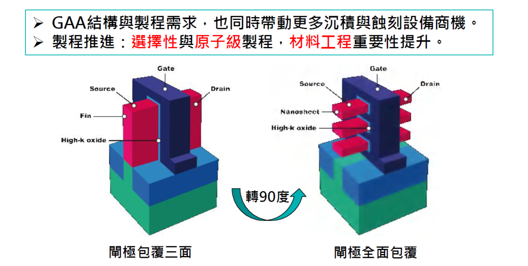
GAA is full-all-around, is a surrounded gate technology transistor, also known as Gaafet. Its concept is presented very early, Dr. Imec Cor Coraeys, Belgium, and its research team published in 1990. GAAFET is equivalent to 3D FinFET's improvement version, the transistor structure under this technique has changed again, the gate and drain are no longer a finish, but a root "small stick", vertically passing the gate vertically That is, so that the gate can achieve four-sided package of the source and drain.
Source: Taiwan Industrial Technology Research Institute
Contrast FinFET, the original source extreme drain semiconductor is fin (FIN), and now the gate is turned into fins. Therefore, GAAFET and 3D FINFET have many similar places on the principles and ideas - this is a great advantage for the wafer factory. From the three contact surface to the four contact surface, and is also split into several quad contact surfaces, it is clear that the gate is further improved by the control of the current.
Compared to the FINFET process, the GAA structure has a larger gate contact area, thereby improving the control capability of the transistor on the conductive channel, and significantly improving the parasitic parameters such as capacitance, thus reducing the operating voltage, reducing the leakage current, reducing power consumption and working. Temperature, thereby facilitating increasing integration to continue to continue Moore Law.
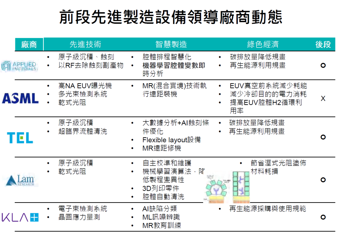
Since the production process required for the new structure is similar to the fin transistors, the key process steps can continue to use existing equipment and technical achievements, which are undoubtedly the lowest technical route replacement scheme for TTEM and Samsung. However, GAA has further improved processing accuracy requirements, requiring regional selective deposition technology and atomic processing capabilities, so material engineering importance is improved, and more deposited and etched equipment business opportunities will also be driven.
Five giants control semiconductor front equipment market
Although more than 80% of the world in 2020 were sold to East Asia, in addition to Japan, China (Continental plus Taiwan) has little influence in equipment industry. The top five major semiconductor fronts (ie, the wafer manufacturing, packaged back to the latter) equipment manufacturers apply materials (ASML), Lam, Tokyo Electronics (TEL) and Keli (KLA) occupied The market share has exceeded 70%, including only Tokyo Electronics Headquarters in East Asia, the rest are American European companies.
Source: Taiwan Industrial Technology Research Institute
Specifically, the application materials are ranked first. Its 2020 is $ 17.2 billion, of which the semiconductor business accounts for 70%. The application material is widely launched on the semiconductor equipment, with the PVD (film deposition) equipment to 38%, and CMP (polishing polishing) equipment accounted for 70%, and the etching equipment accounted for 15%, and ion implantors accounted 67%.
Asa ranked second, 2020, 13.98 billion euros. Aswhera is a photolithography machine, which is currently the only supplier in the EUV (extremely UV) lightning machine, thanks to TSMC, Samsung and Intel's pursuit of advanced technology, 2020 Asak sales 31 The EUV lightning machine has a total of 4.5 billion euros, only 31 EUV photolithography accounts for 32% of its total revenue. Currently, the ASML is jointly developed to develop more refined lithographic processing technologies, such as the introduction of multiple electron beam detection scanning systems in 2020, and limits the interference between the electron beam and the electron beam to 2%, suitable The process of 5 nano nodes. Asa is also working with florescent and IMEC to develop dry photoresist technologies to enhance the EUV resolution and reduce the amount of photoresist. And combined with Lasertec to develop a new generation of EUV mask detection techniques to reduce costs, develop a new generation of EUV masks clean net technology to reduce costs.
Tokyo Electronics 2020 equipment sales is $ 10.37 billion, ranked third. The market share of Tokyo Electronic Polymetled Development Equipment accounted for 91% of the global proportion, and EUV coated developing machines were alone, and the etching machine accounted for 25% of the global proportion of deposits, 27% of cleaning equipment. From 2020 to 2022, Tokyo Electronics Plan invests for 400 billion yen R & D funds, focusing on selective deposition, intelligent etching, supercritical fluid cleaning and other technical directions.
The flin forest semiconductor is received for $ 1050 million, ranked fourth. The floodlin is a global etching equipment leader, of which the memory manufacturing business accounts for 57%, and the logical process is 43%, which is a first five large equipment manufacturers, and the only memory business accounts for more than 50% of the company. As mentioned earlier, flin forests and IMEC in developing EUV dry photoresist technology.
Keli Semiconductor 2020 was received as 5.81 billion US dollars, ranked fifth. Collecting is a global wafer detection equipment leader, with a market share of more than 50%. Keli's stress deformation measurement, multi-beam detection, also puts in force to develop electron beam defect testing techniques for less than 5 nanostructures.
Source: Taiwan Industrial Technology Research Institute
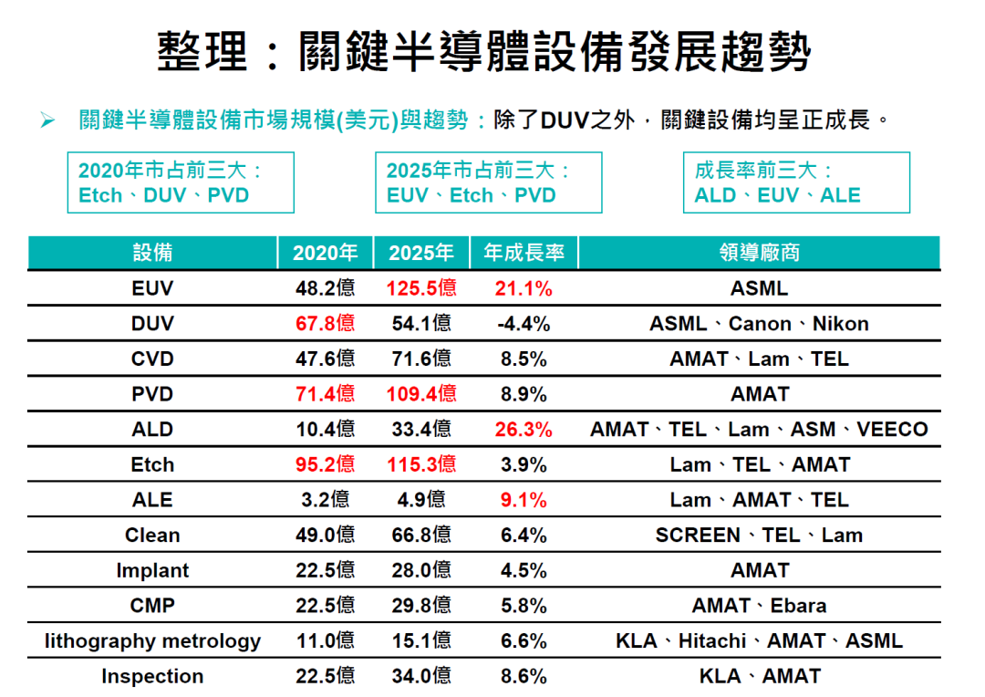
According to the estimation of Taiwan Institute of ITS, global key semiconductor equipment is very good in the next few years. In addition to DUV (deep UV) lithography equipment, the remaining equipment is growing. Among them, ALD (atomic layer deposition) has the highest growth rate. It is expected that the average annual growth rate of 26.3% is expected to be 2020 and 2025, and the EUV equipment growth rate is second, and the average annual growth rate is also two digits. With the amount of EUV equipment, the EUV equipment is expected to reach 12.55 billion US dollars in 2025, which exceeds the etching machine, which has become the highest semiconductor equipment in each sub-directional sales.
Source: Taiwan Industrial Technology Research Institute
China equipment manufacturers have a long way to go
Compared with international manufacturers, the gap between Chinese equipment vendors is large whether it is on sales scale. According to the electronic special equipment industry association data, the sales of domestic semiconductor equipment is 16.182 billion yuan, only about half of the top five guards in 2019 ($ 4.6 billion), the association estimates in October 2020, In 2020, the total sales of domestic semiconductor equipment can be reduced by 21.3 billion yuan, compared with Keli ($ 5.8 billion), it is still less than 60%.
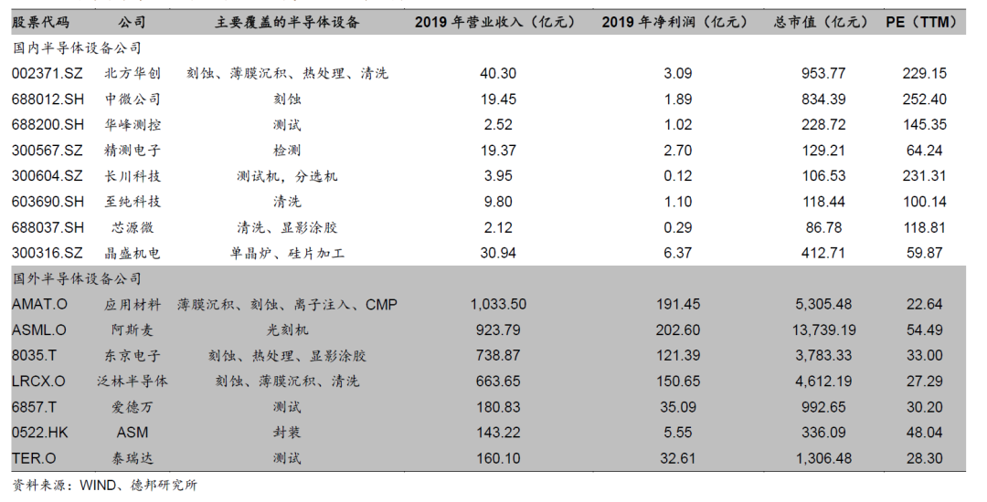
国内外主要半导体设备公司对比(截至2021年1月6日)
资料来源:德邦证券
技术上,我国半导体设备基本还未参与到先进制程(3纳米及以下)研发阶段中,目前也尚不能支持28纳米这样的准主流工艺实现全国产化,大部分国产设备厂商现在能商用的产品还是以成熟工艺产线为主。以社会关注度较高的光刻机为例,国内主要是上海微电子装备有限公司(简称“上海微电子”),上海微电子主流产品还只能满足90纳米、110纳米等制程的光刻工艺要求。
但也有部分领域已经参与到先进工艺竞赛中。比如中微半导体在CCP刻蚀领域已经获得台积电认可,进入其7纳米/5纳米产线;北方华创,则在ICP刻蚀设备上较为出色,28纳米级以上刻蚀设备已经实现产业化,在先进制程方面,硅刻蚀设备已经突破14纳米技术,进入上海集成电路研发中心。
根据《中国制造2025》目标,2020年半导体核心基础零部件、关键基础材料应实现40%的自主率,2025年要达到70%国产化率。但根据长江存储、华力微电子等国内十家晶圆制造企业2017年至2021年一季度的公开招标信息来看,国产化率距离目标还很远。2017至2019年,这十家厂商合计开标4197台设备,其中国产设备为431台,国产化率约为10.3%;而2020年至2021年一季度这十家晶圆厂合计开标1862台设备,其中国产设备达315台,推算目前国产化率在17%,较2017至2019年增长超过6个百分点。
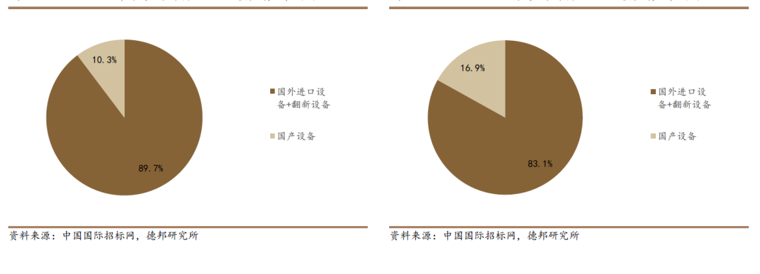
Left: 2017-2019 Ten major crystal round factory equipment localization rate
Right: 2020-2012, Ten Cases, Ten Case Plant, Equipment
Source: Debon Securities
However, domestic semiconductor equipment has also shown very positive changes in the past few years. Technically, enterprises headed by China Micro Semiconductor, Northern Huachang and Yumang Semiconductor, are close to international first-class manufacturers in the field of etching, deposition, dryness, cleaning, ion injection, ion injection. In the market share, some product market share has exceeded 20%, and a strong impact has been launched on the market status of the international semiconductor equipment manufacturers.
It can be seen in the bidding information announced by the Ten Case Circular Factory. In the first quarter of 2017 to 2021, the domestic level rate of dry delay equipment reached 45.5%, while the cleaning equipment (30.6%), etching equipment (22.2%), polishing equipment (21.6%) The domestic system is higher than 20%, and the cos pipe equipment (14.7%) and the glue developing equipment (10.0%) are higher than 10%. The deposition equipment (8.5%) and the front detecting equipment (5.2%) have a low domestic system, only between 5% and 10%, the gap is the larger ion injection machine (2.4%) , The rear test equipment (1.9%) and a photolithography (1.6%).
After entering 2020, domestication rate increased faster. From the top ten wafer factory, it is seen in the first quarter of 2020 to 2021, and the localization rate of polishing equipment, etching equipment, furnace equipment and glue developing equipment has increased by two in 2017 to 2019. number.
From the development trend of global semiconductor equipment industry, with the semiconductor process approaches the physical limit, it is more difficult to develop a new generation of equipment. Taking the EUV lightning machine as an example, in the 1990s, it will be established in the 1990s, and nearly 200 research institutions in more than 40 countries worldwide (Europe contribute more than 100), from basic research, technical research to system integration, The entire R & D system has invested more than 100 billion yuan, surpassing my country's total equipment industry in the past decade.
Yin Zhiyu, chairman of the medium microemicard, also said in the interview with the media, the semiconductor has entered the atomic processing level, and the semiconductor device is manufactured in this precision, and the knowledge and technology of more than 50 disciplines is needed. He pointed out that the plasma etching has been engraved with a few thousand parts of one thousand in diameter of the man, and the accuracy, uniformity and repetition of the hole diameter can reach the tens of thousands of tens of thousands of hair silk. One is one percent. A etching machine processes more than 10 million thin and deep contact holes per year, almost 100% of the holes are fully opened.
Semiconductor devices must not only achieve very fine processing, but most importantly uniformity, stability, repetitiveness, reliability, and cleanliness. As long as you do this, you can meet the core demands of the chip qualified rate. To ensure that the acceptable rate (for example, 90%) requires that each processing manufacturing link has a very high qualification because the current advanced process chip requires 1000 process steps, if each step is 99.9%, Then there is only 36.77% of the final pass rate after 1000 steps.
As a representative of modern intelligent manufacturing, the underlying support of the global information industry, the chip manufacturing is rarely tried to test the opportunity for new equipment manufacturers. After the hard-working development of the sample, only a small part of the development of production equipment, to persuade the wafer manufacturing manufacturer's risk of passing the pass rate and the decline in capacity to help the test are more difficult, Yin Zhizhen said, the prototype is made, Customers are willing to cooperate, but also through at least 80 stringent test projects to finally meet the requirements of the Wafer.
From the historical experience of international manufacturers, the equipment industry should stand stabilize the market, and it is necessary to take a long time to take long-term research and development, consolidate the technical foundation. Such as Yin Zhi, said that the semiconductor equipment requires 50 disciplines, and it is difficult to do not in two bombels. "Magnetic suspension molecular pump in one of the key core components of the semiconductor industry, only two or three people can do, everything needs long-term technology accumulation."
Thanks to globalization, the semiconductor industry has developed to now, but since the Trump government came to the stage, the United States used the semiconductor industry as a weapon, and the technology war for China has seriously affected the supply chain established before the global electronic information industry. Mrouting mechanism. As the most important electronic information industry manufacturing base in the world, the new semiconductor supply chain that is not affected by geopolitic politics is essential, and whenever a technology truly realized a real market breakthrough (for example, 20% market share), "Watts) The corresponding restriction item in the Sena Agreement has lost its meaning. At present, it has a key factor in the effective improvement of the localization rate of equipment, and has become a key factor in the global electronic information industry. China has a rapid expansion of the wafer manufacturing, providing a broad market space and trial error opportunity for domestic semiconductor equipment manufacturers, which is an excellent historical opportunity for domestic semiconductor equipment manufacturers.
mail:wuping@csc-ic.com ; angel@csc-ic.com

right 2023. Chinaic Technology Co. ,Ltd. All Rights Reserved 粤ICP备13001812号